
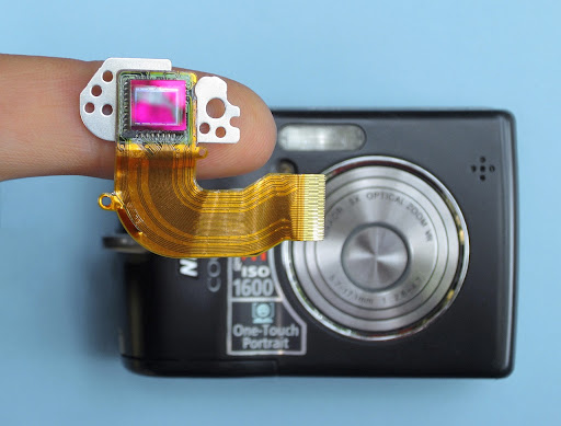
Using a charge-coupled device (CCD) to perform imaging and imaging-related tasks is commonplace in the field of medicine. CCDs are used to produce images of organs and tissues for diagnosis and treatment. However, they can be tricky to use. They can have a noise background in the CCD image, and they store a charge that can be difficult to calculate.
Three shift register phases
Generally, a charge transfer memory comprises four phases. These are a reading register, a storage register, a shift register and a control system. A shift register is a shift one clock pulse ahead of a storage register. In a memory with shift registers, the storage register receives stable data from the shift register, while the control system directs the selected shift clock signal to the device.
A shift register contains a pair of reading electrodes and a storage electrode, each of which is manufactured in a layer of polycrystalline silicon in the third level. These electrodes are located in the insulating layer. An insulating layer is deposited on a semiconductor substrate, and a third layer of polycrystalline silicon is etched onto the electrodes in the layers 41, 43 of the insulating layer.
Each shift register has a transfer electrode adjacent to the reading storage electrode. The transfer electrode is made in a layer with a second type of doping, while the reading storage electrode is made in a layer with essentially no doping. The doped zone is the same as the doped zone in the reading register.
The transfer electrodes are supplied with clock signals through clock signal lines. Charges are transferred from the potential well P4 in the shift register to the potential well PO in the storage register. The potential well PO has a value that is lower than the value of the memory’s transfer potential, VC. This lower value prevents electrons from returning to the shift register.
The transfer electrodes are arranged in series. These electrodes are also connected through connection wires to supply sources. Cyclic voltages are applied to the electrodes of each group in the shift register. These voltages are controlled to a low and high level, with the extreme values being the same as the extreme values of the voltage V1 applied to the first electrode of the shift register.
In charge transfer memory, the reading register is parallel to a second direction, and is preferably perpendicular to the first direction. Charges are transferred through the potential well P4 in the shift register to the potential well PO in the storage register.
Quantification of stored charge in CCD photodiodes
Optical multichannel analyzers are devices that record the spectrum, convert the incoming stimulus into a physical signal, and display the results in real time. They are usually designed with a dispersing arrangement that produces a diffraction-free beam. These devices are useful in quality assurance and research laboratories. They are particularly useful in the area of multi-channel spectroscopy. They have a small footprint, low dark currents, and are highly compatible with existing laboratory equipment. They are available in the usual compass sizes, from small single-channel models to large three-dimensional arrays.
A multichannel detector is the modern incarnation of the old standby, the diode. A diode is a semiconductor chip that enables light to pass through it. Electrons in the semiconductor conduction band are swept from one side of the chip to the other by the force of an external electric field. They are then read out with an imaging tube. A multichannel spectrometer is similar in function, with the added advantage of a higher resolution and longer measuring time. The largest limitation to the multichannel device is the size of the silicon chip. This limitation is mitigated by a high-intensity light source.
The best multichannel detector is one that is able to record the entire spectrum from a dispersing array. The trick is to find the optimal configuration for your application. This can be achieved by using a well-matched light source, a suitable reference wavelength, and choosing a diode with a suitable size and shape. Some detectors are designed with a multichannel grating to reduce the number of detectors, while others feature a multichannel array for increased spectral resolution. They are useful in a number of applications, including determining the source of a fluorescently labeled material, or measuring the spectrum of a liquid with a high concentration of impurities. A multichannel spectrometer is also the cheapest of all the options, making it a cost effective and high quality instrument for research purposes. These devices are most useful when multiple channels are needed, or when the wavelengths of interest are dispersed in an unsupervised manner.
Noise background in the CCD image
Normally, a CCD imaging system works in two phases, namely the exposure and the readout phase. The exposure phase is the time that a CCD is exposed to the light and the readout phase is the time that the photon signal is extracted from the CCD. Both phases are important for the overall performance of a CCD imaging system.
The first source of noise in a CCD imaging system is photon noise. Photon noise is produced from statistical variation in the arrival rate of photons on the CCD. This noise is also referred to as shot noise.
Another source of noise in CCD imaging systems is dark noise. This noise is produced from statistical variation in the number of thermal electrons that are generated within the silicon structure of the CCD. The rate of dark current is also a function of the temperature of the device. Common techniques to reduce dark current are cryogenic refrigeration, thermoelectric cooling, and special device fabrication techniques.
In high performance CCD cameras, the dark current is typically cooled to a minimal level like Neuromorphic Camera with better temporal resolution. This reduces the overall dark current and increases the signal-to-noise ratio. The dark current is reduced by half for every 5 to 9 degrees Celsius.
There are three main noise sources in a CCD imaging system. Each noise source must be considered in calculating the signal-to-noise ratio. These sources are photon noise, dark noise, and read noise.
The signal-to-noise ratio (SNR) is the ratio of the measured light signal to the combined noise. SNR is a very important measure of the quality of a measurement system. It is especially important for high quality digital images and accurate measurements of light. The SNR can be calculated as a per-pixel basis or as a relative magnitude.
The SNR can be calculated by combining the signal generated by neighboring pixels into a larger pixel. A modified equation is shown below. It combines the signal generated by the neighboring pixels, assuming that the same signal is present in each pixel within the group.
The gain probability at each stage of the register is typically N>500. This probability is increased by using a faster readout speed.

An author of BlogMandi, We have published more articles focused on blogging, business, lifestyle, digital marketing, social media, web design & development, e-commerce, finance, health, SEO, travel.
For any types of queries, contact us on blogmandi.info@gmail.com